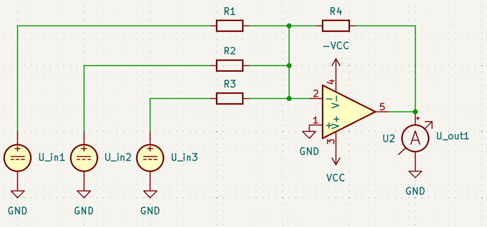
To analyze this circuit, the operational amplifier is assumed to be ideal, meaning:
In these formulas, \(I_{Rx}\) represents the current flowing through \(R_1\), \(R_2\), \(R_3\) or \(R_4\).
\(U_D\) is the voltage difference between the non-inverting (+) and inverting (-) terminals.
\(U_{inx}\) and \(U_{out}\) are the input and the output voltages, respectively and \(U_{+}\) and \(U_{-}\) are the non-inverting and inverting input voltages of the opamp.
$$ U_D = 0 $$ $$ -I_{R4} = I_{R1}+I_{R2}+I_{R3} $$ $$ -{U_{out} \over R_4} = {U_{in1} \over {R1}}+ {U_{in2} \over R_2} + {U_{in3} \over R_3} $$ $$ U_{out} = -{{U_{in1} \over {R1}}+ {U_{in2} \over R_2} + {U_{in3} \over R_3}} *R_4 $$ These formulas illustrate the calculation of the output voltage. By selecting \(R_1\) = \(R_2\) = \(R_3\) = \(R_4\) the amplification factor becomes 1 and the circuit functions as an inverting adder.
- The differential input voltage \(U_D\) is zero, implying no input offset voltage.
- The output offset voltage is zero.
- The input current is negligible (zero). / The input resistance is infinite.
- The output resistance is zero.
- The open-loop gain is infinite.
In these formulas, \(I_{Rx}\) represents the current flowing through \(R_1\), \(R_2\), \(R_3\) or \(R_4\).
\(U_D\) is the voltage difference between the non-inverting (+) and inverting (-) terminals.
\(U_{inx}\) and \(U_{out}\) are the input and the output voltages, respectively and \(U_{+}\) and \(U_{-}\) are the non-inverting and inverting input voltages of the opamp.
$$ U_D = 0 $$ $$ -I_{R4} = I_{R1}+I_{R2}+I_{R3} $$ $$ -{U_{out} \over R_4} = {U_{in1} \over {R1}}+ {U_{in2} \over R_2} + {U_{in3} \over R_3} $$ $$ U_{out} = -{{U_{in1} \over {R1}}+ {U_{in2} \over R_2} + {U_{in3} \over R_3}} *R_4 $$ These formulas illustrate the calculation of the output voltage. By selecting \(R_1\) = \(R_2\) = \(R_3\) = \(R_4\) the amplification factor becomes 1 and the circuit functions as an inverting adder.