HDMI Background Information

HDMI (High-Definition Multimedia Interface) is a digital video and audio interface that is electrically compatible with DVI. Its development began around 2002, and over the years, HDMI has evolved to support various resolutions and color formats. It is widely recognized for its Type A receptacle (shown on the right), and newer HDMI revisions can handle display resolutions exceeding 8K.

HDMI Interface Design Basics

To design a basic HDMI controller, two key signals must be considered: the TMDS data lines and the TMDS clock signal. TMDS (Transition-Minimized Differential Signaling) is a specialized 8b/10b encoding algorithm designed to minimize signal transitions between 0 and 1, ensuring robust signal integrity. This encoding process adds two extra bits to the original 8-bit color data, making it more resistant to noise and transmission errors.
This core will implement TMDS encoding in RGB format to maintain compatibility with the DVI standard.

Data Transmission Process

To transmit video data over HDMI:
  1. The parallel RGB color data must be TMDS encoded.
  2. The parallel TMDS data must be serialized.
  3. The serialized TMDS data can be transmitted.
In this design, the data is loaded in parallel and then serialized, allowing most of the system to operate at a lower clock frequencies.

Video Timing Considerations

The video timing requirements for HDMI are largely similar to those of a VGA timing controller. However, a key difference is that the back porch and front porch regions, which were essential in VGA for CRT displays, are no longer technically required in HDMI. Instead, these intervals can be utilized for transmitting additional data, such as audio signals.

VHDL Design

The implemented controller entity, shown on the right side, features six inputs and two differiential outputs.

Inputs:

Outputs:

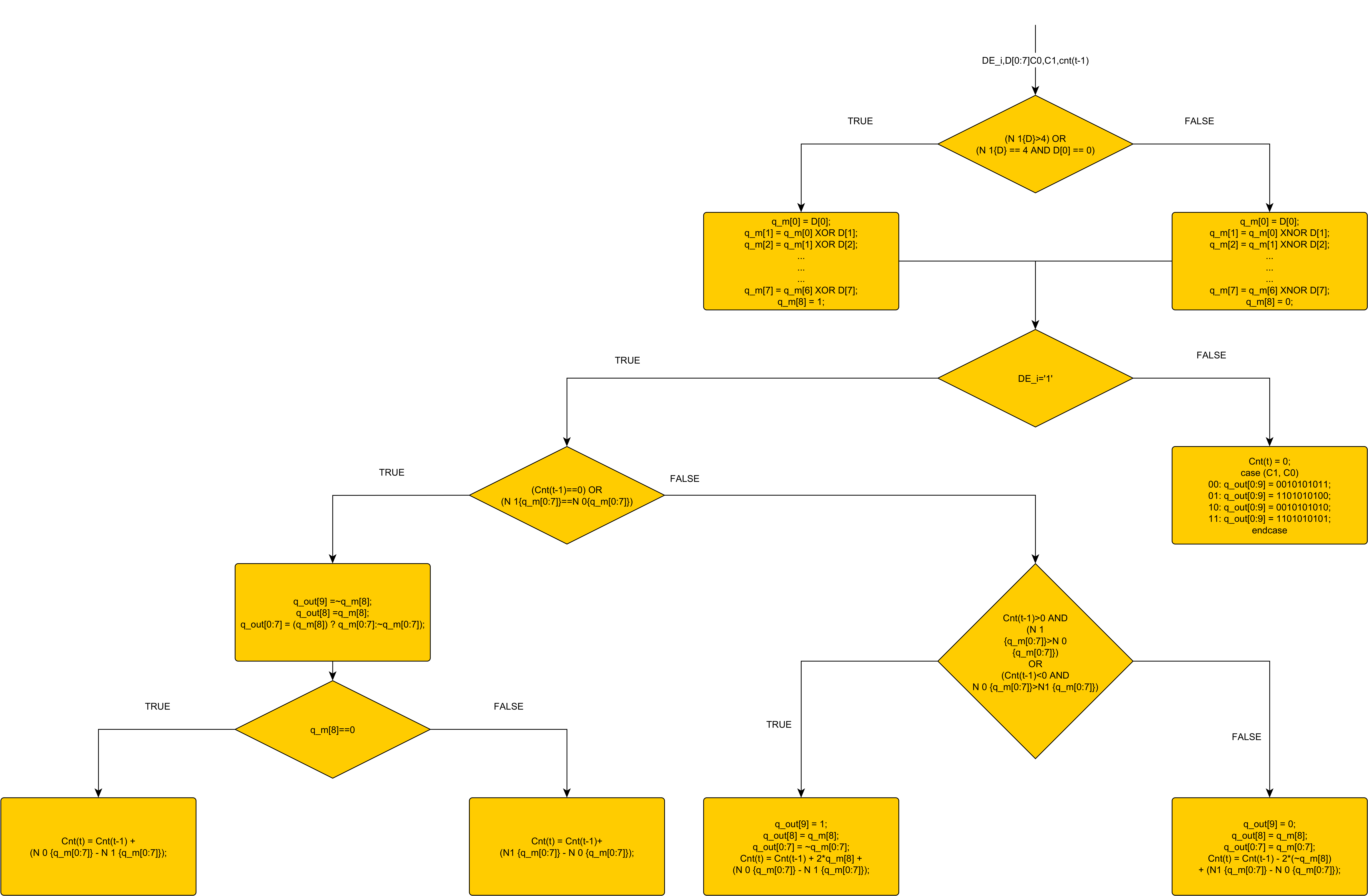
The design primarily consists of three key components: the TMDS encoder, the parallel-to-serial shift registers, and the timing counters. The TMDS encoders operate according to the DVI specification and include functions designed for simplified integration. The functional diagram of the encoder architecture is shown in the following image.


Parametrization:

The core is designed for a fixed output frequency, which can be configured using generic parameters. The key parameters are listed below:
      
        GENERIC
(
-- VGA timing definitions in pixels
h_visible_area : INTEGER := 800; -- Number of visible horizontal pixels h_frontporch : INTEGER := 40; -- Horizontal front porch width h_sync_pulse : INTEGER := 128; -- Horizontal sync pulse width h_back_porch : INTEGER := 88; -- Horizontal back porch width h_whole_line : INTEGER := 1056; -- Total horizontal pixels v_visible_area : INTEGER := 600; -- Number of visible vertical lines v_frontporch : INTEGER := 1; -- Vertical front porch height v_sync_pulse : INTEGER := 4; -- Vertical sync pulse height v_back_porch : INTEGER := 23; -- Vertical back porch height v_whole_line : INTEGER := 628 -- Total vertical lines );
Using these generic parameters, the core generates appropriate timing signals for the display. The source code for this module can be found on Github . Additionally the source for the timing generator can also be found at Github .

Testbench:

To create a fully integrable design and verify its functionality, a testbench was developed. This testbench, along with its Makefile for GHDL, is also available on Github . The testbench simulates the VGA core and the parallel to serial shift register. This ensures the generation of valid timing signals and a correct tserialisation process.